See how sound waves shape laser pulses and deliver faster throughput without sacrificing accuracy and quality.
You build the most innovative PCB boards in the world with demanding accuracy and yield requirements. New trends in miniaturization demand ultra-fine vias, high-density layouts need precise drilling, and innovative materials within complex multi-layer stack designs pose unique drilling obstacles. Will your current systems meet the demands of the increased device complexity driving Advanced Packaging innovation?
For PCB manufacturers of HDI boards, CO2 laser processing is the optimal choice for overall lower cost of ownership. ESI leverages our expertise in laser processing and our proven track record of success in flexible PCB manufacturing with laser-based systems, and applies it to the HDI manufacturing segment. Our solutions are engineered to provide great reliability at high-quality output with the industry’s lowest cost of ownership, and backed by ESI’s professional service and support organization with local offices through the world.
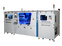
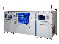
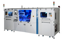
A CO2 laser solution for HDI via drilling that leverages ESI’s expertise for PCB and substrate processing
Are your current CO2 systems ready to optimize your production?
Discover innovative technology features for smaller vias, faster throughput, and higher accuracy to meet your precise production demands. Let Geode’s innovative capabilities maximize your capacity and elevate YOUR production.
Take advantage of our powerful new CO2 laser and a new set of control capabilities. Leverage ESI’s decades of laser-material interaction experience and application expertise to innovate and stay ahead.
- HDI PCB Manufacturing
- Integrated circuit packaging
- Substrate processing
- System level packaging
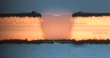
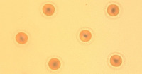
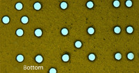
High Density Interconnect (HDI) PCB Base Material via Drilling Examples
ESI’s HDI systems enable PCB manufacturers to drill vias in a broad range of copper-clad base materials such as glass-woven reinforced epoxy resins (FR4) or other specialty materials.
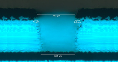
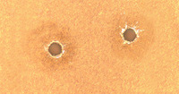
Integrated Circuit Packaging (ICP) Base Material via Drilling Examples
Discover the innovative technology features to meet your precise production demands.
- Precision Power Control for ultra thin materials
- High Diameter Integrity and low OH with AcceleDrill
- Hypersonix Intra-pulse drilling – One-shot recipe for maximum throughput
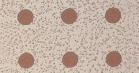
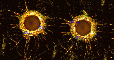
CO2 Via Drilling for Glass-woven Reinforced Epoxy Resins (FR4)
The Geode system enables High density interconnect (HDI) PCB fabricators to incorporate into production a wider range of materials, from copper-clad base materials to glass-woven epoxy laminates (FR4) and others. With innovative CO2 laser technology, new control capabilities and applied expertise gained through decades of engineering leadership in flex, combine to deliver breakthrough levels of accuracy, throughput and yield.
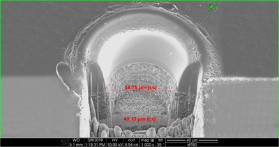
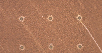
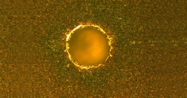
CO2 Via Drilling For Flip Chip Ball Grid Array (FCBGA) Base Materials
The Geode A laser drill system combines special laser/optics configuration with precision pulse shaping and steering specifically designed for ABF materials. Geode’s technology enables a greener manufacturing solution through 21% less floor space 72% less weight and up to 65% less power consumption than the competition. The combination of QCW laser and AOD technology also ensures highest throughput and lowest cost of ownership for our customers.
Rigid PCB Laser System Guide
 Geode |
 Geode G2 |
 Geode A |
 Geode X |
|
|---|---|---|---|---|
| Overview | HDI microvia drilling solution for precision processing of your HDI, SLP and ICP applications. | ESI’s next generation HDI microvia drilling solution for precision processing of your HDI, SLP and ICP applications. | The industry’s most Innovative CO2 via drilling system powered by quasi-continuous wave laser and AOD technology for advanced substrate applications. | Optimized for small via geometries at the highest productivity. Built for the lowest cost of ownership. Designed for the most advanced material. |
| Target Applications | Geode S: SLP, mSAP, HDI Geode L: HDI |
Geode G2 VS: SiP, FCCSP, FCGBA, mSAP Geode G2 S: SLP, mSAP, HDI Geode G2 L: HDI |
FCBGA, IC Substrate | IC Substrate |
| Target Via Range | Geode S: 35-90 um Geode L: 60-200 um |
Geode G2 VS: 28-75 um Geode G2 S: 35-90 um Geode G2 L: 60-200 um |
30-85 um | 10-35 um |
| Max Via Size | Geode G2 VS: 200 um Geode G2 S: 300 um Geode G2 L: 500 um |
|||
| Total System Accuracy | Geode S: ±8 um |M| + 3σ Geode L: ±10 um |M| + 3σ |
Geode G2 VS: ±8 um |M| + 4σ Geode G2 S: ±8 um |M| + 4σ Geode L: ±10 um |M| + 4σ |
<7 um |M| + 4σ |
<4um|M| + 4σ (glass master) |
| Laser Pulse Frequency | Up to 6.5 kHz | 200 kHz QCW | ||
| Peak Power | 2.5 kW | |||
| Energy Monitoring | Real time pulse energy monitoring (programmable alarm settings) | |||
| Footprint | 21% less floor space and 72% less weight versus the competitor | |||
| Availble Load/Unload Automation | Standard, Standard with NG Function, Panel Flipper with NG Function | |||
Resources
Geode Data Sheet(455.8 kB, PDF) Geode A Data Sheet(601.5 kB, PDF) Laser Direct Drilling (LDD) Comformal Mask Processing Non-Copper Clad Dielectric Material Via Drilling Inside Making a Via with Geode™: Hypersonix™ Edition(1:59) Inside Making a Via with Geode™: AcceleDrill™ Edition(2:13) Inside Making a Via with Geode™: RTPC Edition(2:39)