Non-Copper Clad Dielectric Material Via Drilling
Dielectric materials where no copper cladding is required during lamination are typically used in semi-additive plating, modified semi-additive (mSAP), MLCC, or other such applications.
Are you ready to elevate your non-clad processing?
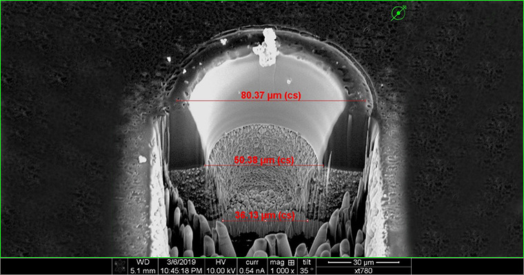
Example Materials
- ABF
- Green sheet (LCC)
- Ceramic (Si3N4)
Process Limitations
- Non Cu-clad applications typically require low power, long pulse width laser profiles
- There can be some throughput limitations (depending on applicable Geode configuration and via specs)
- Material handling (limited protection)
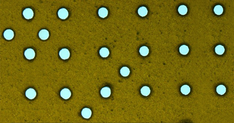
Advantages
- Low power
- High throughput (depending on application)
- More consistent via geometry (no glass fibers)
- Low damage to bottom Cu
 Ultra-High Velocity