
Geode X UV Laser via Drilling System
Geode X UV Laser via Drilling System
Optimized for small via geometries at the highest productivity.
Built for the lowest cost of ownership.
Designed for the most advanced materials.
- High precision and high-speed IC substrate manufacturing
- AcceleDrill™: Drill multiple via diameters in a single pass
- HyperSonix™: Precise power control to optimize via formation See All Features
Specifications
- Wavelength355 nm
- Pulse Rate1 MHz
- Average Power20 W
- Panel ProcessingDual-head two panel system
- Panel Size510x610 mm (Maximum)
- Panel Height DetectionLaser displacement sensor
- Part Thickness Range50 to 3000 μm
- Energy MonitoringReal time pulse energy & monitoring (programmable alarm settings)
- Load / Unload AutomationStandard, Custom to order
- Total System Accuracy<4μm |M| + 4σ, glass master
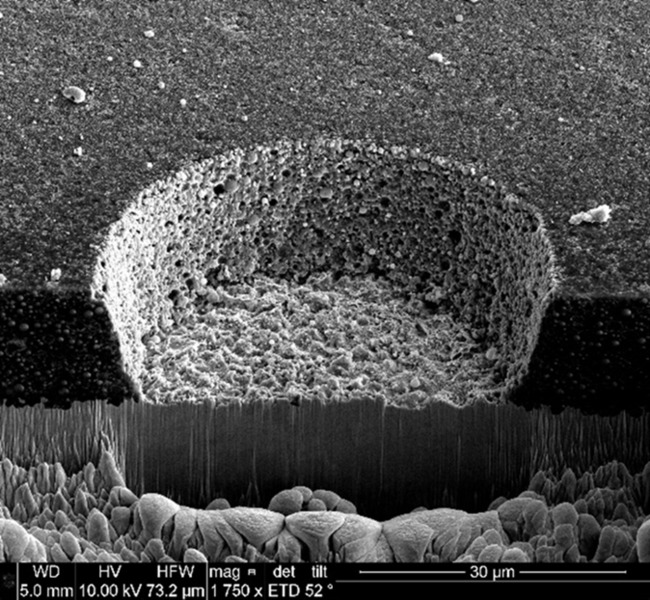
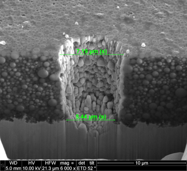
- Via Diameter Range10 to 90 μm (typical)
Features
The World’s Most Advanced Small Via Drilling System
UV Laser Technology enables smaller focus beam sizes to drill smaller via geometries for High Precision and High-Speed IC Substrate Manufacturing. Geode platform technology enables a greener manufacturing solution through reduced floor space, weight, and power consumption compared to traditional laser drilling tools.
AcceleDrill™ Spatial Distribution in Action
Improves productivity by allowing a single pass over a panel without having to switch between different optical configurations to control via geometry. Geode™ will enable you to process an extensive dynamic range of via size without changing the spot size.
HyperSonix™ Time & Power in Action
Your traditional Rigid PCB via drilling systems may need several sequential process steps in order to optimize ablation in a traditional material stack. Increase your throughput and accuracy with Geode’s real-time pulse control capability to optimize the material ablation process.
RTPC - Monitor & Control in Real Time
Discover how you can increase stability and via quality with the industry’s only real-time power control. Geode™ will enable you to actively manage power fluctuation to ensure higher productivity in your Rigid PCB processing.
LiteDesign™
Footprint - Compact and lightweight system architecture allows for more flexibility in system placement and use on production floor.
VDC™
Accuracy - Via density compensation improves via diameter stability, accuracy and throughput.
UpTime™
Easy-access design improves serviceability, decreasing maintenance and service downtime.
Processes
-
IC Substrate
Materials
- Ajinomoto Build-Up Film® (ABF)
- Pre preg material (PPG)
- Resin-Coated-Copper (RCC)
- Solder Resist
Solder Resist via Example
ABF via Example
 IC Substrates")

