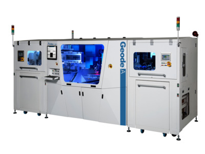
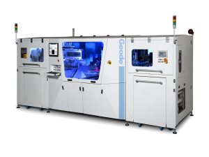
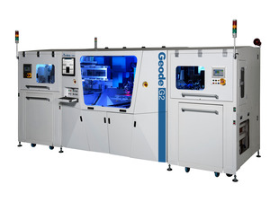
Geode™ A CO2 Via Drilling System For FCBGA (ABF) IC Substrates
Overview
Optimized for productivity.
Built for the lowest cost of ownership.
Designed for the most advanced materials.
- High precision and high-speed FCBGA ABF IC substrate manufacturing
- AcceleDrill™: Drill multiple via diameters in a single pass
- HyperSonix™: Ablate copper and material with minimal pulses
Products
Features
The world’s most advanced ABF via drilling system
CO2 Laser System for High Precision and High-Speed ABF IC Substrate Manufacturing. Geode’s technology enables a greener manufacturing solution through 21% less floor space 72% less weight and up to 65% less power consumption than the competition.
AcceleDrill™ Spatial Distribution in Action
Outpace your competition by increasing your Rigid PCB throughput by drilling multiple via diameters in a single pass. Geode™ will enable you to process an extensive dynamic range of via size without changing the spot size.
HyperSonix™ Time & Power in Action
Your traditional Rigid PCB via drilling system may need several pulses to ablate copper & material, reducing your production yield. Increase your throughput and accuracy with Geode’s pulse chopping capabilities to ablate copper and material with minimal pulses.
RTPC - Monitor & Control in Real Time
Discover how you can increase stability and via quality with the industry’s only real-time power control. Geode™ will enable you to actively manage power fluctuation to ensure higher productivity in your Rigid PCB processing.
LiteDesign™
Footprint - Compact and lightweight system architecture allows for more flexibility in system placement and use on production floor.
VDC™
Accuracy - Via density compensation improves via diameter stability, accuracy and throughput.
BCT
The MKS beam characterization tool offers precision in-line laser/optical evaluation and control for improved calibration and via consistency.
UpTime™
Easy-access design improves serviceability, decreasing maintenance and service downtime.
Materials
- Ajinomoto Build-Up Film® (ABF)
- EMC
- Resin-Coated-Copper (RCC)
- Non CU-Clad Dielectric
Processes
- Advanced HDI PCB
- IC Packaging
- IC Substrate
Specifications
-
Average Power>250 W
-
Peak Power100 W
-
Panel ProcessingDual-head two panel system
-
Panel Size Range16x20 in. to 22.05x24.5 in.
-
Panel Height DetectionTouchdown sensor (calibrated to align with camera focus), Z-Mapping
-
Part Thickness Range50 to 3000 um
-
Energy MonitoringReal time pulse energy & monitoring (programmable alarm settings)
-
Automation Accuracy(panel to chuck): 500 um
-
ProcessingLDD Conformal Mask
-
Scan Area12 x 6 mm
-
Load / Unload AutomationStandard, Standard with NG Function, Panel Flipper with NG Function
-
Total System Accuracy<7um |M| + 4σ
-
Via Diameter Range30 to 85 um
-
Laser Pulse Frequency200 kHz (No rep rate)


 Ultra-High Velocity